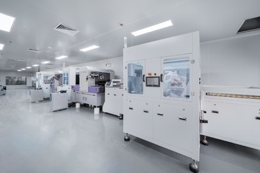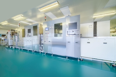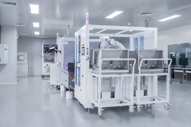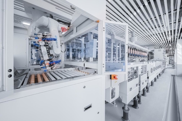
HOREXS Group was located in CHINA mainland,has three subsidiaries:Boluo HongRuiXing Electronics Co., Ltd(Located in Huizhou city GuangDong),HongRuiXing (HuBei) Electronics Co.,Ltd(Located in HuBei province),Horexs Electronics (HK) Co.,Ltd(Located in HK),All are just located in difference place to meet our customers demand of ic substrate manufacture.Horexs supplies different kinds of IC substrate products. High quality and favorable price. We're pleased to get your Inquiry and we will come back to as soon as possible. We stick to the principle of "quality first, service first, continuous improvement and innovation to meet the customers" for the management and "zero defect, zero complaints" as the quality objective. To perfect our service, we provide the products with good quality at the reasonable price.
HOREXS Huizhou Built in 2009
Capacity 15000sqm/Month,Tenting process,BT materials,L/S 35/35um,
Mainly memory(BGA) substrates,parts of MEMS/CMOS/MiniLED/Sip/FCCSP package substrates and others ultra thin substrate.
HOREXS Hubei Built in 2020
HOREXS-Hubei is committed to the development of IC substrate in China, striving to become one of the top three IC substrate manufacturers in China, and striving to become a world-class IC board manufacturer in the world . Technology like L/S 20/20un,10/10um.BT+ABF materials. Support: Wire bonding Substrate Wire bonding(BGA) Substrate Embedded (Memory IC substrate) MEMS/CMOS,Module(RF,Wireless ,Bluetooth) 2/4/6L (1+2+1/2+2+2/1+4+1),Buildup(Buried/Blind hole) Flipchip CSP; Others ultra ic package substrate.
Horexs is a professional advanced semiconductors electronics packaging material manufacturer of semiconductor packaging substrate; Horexs's Products are widely used in IC assembly&Semiconductor package(Sip/CSP/FCCSP/PBGA/LGA/FBGA/MEMS/CMOS/RF Module etc).Such as Micro SD substrate,Sensor substrate,FCCSP package substrate,Fingerprint card substrate and other ultra thin substrate.
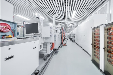
Horexs was founded in 2010, a total investment of ten million yuan, now has more than 20 professional technical personnel, engineering management and technical personnel more than 100 be trained with regularity, the monthly production capacity of 3000 square meters, plant a total area of 10000 square meters, including printing, electronic measurement, testing workshop dust-free workshop according to the construction of high standard; In order to meet the needs of high precision circuit board configuration Hitachi high-speed drilling machine, automatic electroplating production line, printing, exposure, development, etching, laminated, gold, gold, high standard NC a full set of production equipment; To ensure that the product qualified rate one hundred percent, electrical measuring machine, flying probe test, testing equipment for physical or chemical analysis room; Set up sewage treatment station and environmental protection exhaust gas treatment system, the heavy metals by ion exchange of organic waste water, complex, activated carbon filtration, chemical precipitation method to realize effective treatment discharge standards and a series of advanced technology.
Horexs adhere to high quality products, fast delivery, perfect service, good reputation, flexible marketing as the foundation of the market competition; To win in the Pearl River Delta and overseas customers trust and support. Also look forward to working with our new customer cooperation, achieve a win-win situation, create a better future!

Horexs' mission is that to help customers save cost by our advanced technology,Continously provide the best technology.
In 2009,Horexs factory was built in Boluo disctrict ,Huizhou city CHINA;(Nearby Shenzhen city)(12000sqm output monthly)
In 2010,Horexs factory start produce memory ic package substrates;
In 2012,Horexs realised 80% products are memory card/IC substrate board,with 50um sapce;
In 2014,Horexs start to R&D MiniLED/MEMS package substrate products;
In 2015,Horexs manufacture capability reach to 10000sqm monthly;
In 2017,Horexs imported more LDI/Mekki Laminate press machines from Japan;
In 2019,Horexs decided build second factory in hubei province;
In 2020,Horexs built SZ office,mainly serve for international business,same time,second factory start buidling;
In 2022,Horexs Hubei factory running 1st stage in July,Built relationship with SPIL;
In the future,Horexs will focus more on IC substrate IC assembly IC package pcb ,and put more in our R&D team.We never stop our technology improvement,Because Horexs always win customers by technoloy.
IC substrate (2layer or Multilayer) manufacture/Support OEM/ODM.Including IC assembly/IC package substrate(BGA/Flipchip/Sip/Memory Package substrate) pcb board.All kind of memory card pcb board,UDP/eMMC/MEMS/CMOS/Storage designing and testing pcb boards,5G electronics thin FR4 circuit boards,Medical electronics thin pcb boards,SIM card/IoT electronics /Sip package substrate circuit boards,Sensor package substrate pcb,and others ultrathin pcb substrates.
Memory (BGA)
MicroSD (T-Flash) Card is a memory card that is optimized for mobile device and is used for high-tech digital device such as Smart Phone, DMB Phone, PDA and MP3 Player etc. Its size is about one third of SD Card and it can be compatible with SD card by using additional adapter.


Nand /Flash Memory substrate like eMMC/MCP/UFS/DDR/LPDDR,MicroSD/TF/Dram substrate;
Wire bonding package,ENIG /soft&hard gold;
Welding ink leveling process;
Features
Thin PCB (>0.08mm)
High-Stack Technology
Wafer thinning : > 20um (Thin DAF : 3um)
Chip Stack : < 17 Stack
Thin die handling : Dedicated D/A Ejector
Long wire & Overhang Control (Au – 0.7mil)
Compression molding system
Eco-Friendly Green Compound EMC
Saw Singulation & PKG Grinding
Substrate : 0.21um Matrix Type Substrate
Die Attach Adhesive : Non-conductive DAF or FOW
Gold Wire : 0.7mil (18um) Gold Wire
Mold Cap : Green EMC
Temperature Test : -40℃ (168h)/ 85℃ (500h)
Moiture and Corrosion Test : 40℃/ 93% relative humidity (500h), Salt water spray 3% NaCl/35℃ (24h)
Durability Test : 10,000 mating cycles
Bending Test : 10N
Torque Test : 0.10Nm, +/-2.5° max.
Drop Test : 1.5m free fall
UV Light Exposure Test : UV 254nm, 15Ws/㎠
Sip


System in a package (SiP) or system-in-package is a number of integrated circuits enclosed in one or more chip carrier packages that may be stacked using package on package.The SiP performs all or most of the functions of an electronic system, and is typically used inside a mobile phone, digital music player, etc.Dies containing integrated circuits may be stacked vertically on a substrate. They are internally connected by fine wires that are bonded to the package. Alternatively, with a flip chip technology, solder bumps are used to join stacked chips together. A SiP is like a system on a chip (SoC) but less tightly integrated and not on a single semiconductor die.
SiP dies can be stacked vertically or tiled horizontally, unlike less dense multi-chip modules, which place dies horizontally on a carrier. SiP connects the dies with standard off-chip wire bonds or solder bumps, unlike slightly denser three-dimensional integrated circuits which connect stacked silicon dies with conductors running through the die.
Package: compatible with BGA, LGA, Flip Chip, Hybrid solutions etc.
Surface treatment: Soft Au, ENEPIG, ENIG, SOP, OSP
Excellent performance: fine impedance line width control, excellent heat dissipation performance
RF/Wireless: Power amplifiers, baseband, transceiver modules, Bluetooth TM, GPS, UWB, etc.
Consumer: Digital cameras, handheld devices, memory cards, etc.
Networking/Broadband: PHY devices, line drivers, etc.
Graphics processors -. TDMB -. Tablet PC -. Smart phone
Features
High Density SMD
Passive Component (≥ 008004)
SAW,BAW filter, X-tal, Oscillator, Antenna
EPS (Embedded Passive Substrate)
EAD (Embedded Active Device)
Core & Coreless Substrate
MCM, Hybrid (F/C, W/B)
Double Side Mount (F/C, Passive Component)
Double Side Molding
Mold Grinding
Double Side Solder Ball Attach
EMI Shielding
Moisture Sensitivity : JEDEC Level 4
Unbias HAST : 130℃, 85%RH, 2atm, 98Hrs
Temp. Cycling : -55℃/+125℃, 1000 cycles
High Temp.Storage : 150℃, 1000Hrs
Module


Build-up layer:4 layer;
Line/space (Min):35/35um;
Total board thickness (Min.):0.25mm(HDI type)
Our base material is of an optimum type and thinness to meet the requirements of module-mounted products for compactness and high functionality and to enable the micro-fabrication development necessary for the high-density wiring/land size reduction required by such boards.
Board thickness 0.25mm (4 layered) achieved by the adoption of ultra- thin base material/prepreg
High-reliability thinner board suited for any type of layer connection structure
Plating technology creates an optimum product for side connection on module
Camera modules
Bluetooth modules
Wireless modules
Power amp modules
MEMS/CMOS


Micro-electromechanical systems (MEMS) is a process technology used to create tiny integrated devices or systems that combine mechanical and electrical components. They are fabricated using integrated circuit (IC) batch processing techniques and can range in size from a few micrometers to millimetres.
Build-up layer:2/4/6 layer
Application:Mobile industry(Camera sensors),Industrial Automotive car sensors,Security industry
Flipchip/BGA/CSP (2023-HOREXS roadmap development)


An IC wafer having convex contacts is inversely attached to a carrier Substrate, which is called Flip Chip Substrate, as a buffer interface for the electrical connection and transmission between the wafer and the circuit board, to determine the Logic of the wafer through the Fan out function of the carrier Gate output can reach the maximum number of inputs to the logic gate on the circuit board. The difference with the hit-line carrier is that the connection between the chip and the carrier is Solder bumps instead of Gold wire, which can greatly improve the signal density (I/O) of the carrier Port), and improve the performance of the chip, as the trend of future onboard development
FC-BGA (flip chip ball grid array) on a high density semiconductor package substrate allows high speed LSI chips with more functions.
FC-CSP(Flip Chip-CSP) means that the chip mounted in the PCB is turned over. Compared to the general CSP, the difference is that the connection between the semiconductor chip and the substrate is not wire bonding, but bumps. Since it does not require Wire-Bonding, it is much smaller than those products that go through the general wire bonding process. In addition, many chips and the PCB are connected at the same time, in contrast to wire bonding, which requires you to connect one at a time. Moreover, the connection length is much shorter than in wire bonding, so the performance can be improved.
The fcCSP package is the main platform in flip Chip package family, which also includes bare die type, Molded (CUF,MUF) types, SiP types, Hybrid (fcSCSP) types and a package subsystem meeting the standard BGA footprint that contains multiple components within the same package (MCM fcCSP). Options also include configurations with thin core, Pb-free and Cu Pillar bump and process method (Mass reflow, TCNCP).The Flip chip CSP packages are suitable for low lead count, high frequency, high performance, and portable products such as performance memory, RFICs, and DSPs.
Line/Space:15/15um&20/20um.
Process:Msap/Sap/Additive.
Surface finished:ENEPIG/Slective OSP etc.
Application:Network,CPU,Automotive,SOC,Gpu etc.
Features
Substrate Layer : 4 ~ 8 Layer
Bump pitch : Min.130um (Solder bump)
Cu Pillar (TCNCP ≤ 50um / Mass Reflow ≥ 65um)
Die size : 0.8~12.5mm
Package size : 3~19mm
PCB : BT or Equivalent (2~6 Layer)
Bump : Eutectic, Pbfree, Cu Pillar
Flux : Water Soluble
Underfill : Epoxy
EMC : Green (Low Alpha)
Solder ball : Sn3.0Ag0.5Cu (Standard)
Marking : Laser
Packing : JEDEC Tray
Moisture Sensitivity : JEDEC Level 3
Unbias HAST : 130℃, 85%RH, 2atm, 98Hrs
Temp. Cycling : -55℃/+125℃, 1000 cycles
High Temp.Storage : 150℃, 1000Hrs
Micro/MiniLED Substrate


Mini LED refers to LED chip with size of 100μm. The size is between small spacing LED and Micro LED. It is the result of further refinement of small spacing LED. Among them, the small spacing LED refers to the LED backlight or display product with the distance between adjacent lamp beads below 2.5mm.
The Mini LED has a better display effect, an order of magnitude increase in response speed, and the screen can be thinner and thinner, with a significant reduction in power consumption.With extended battery life, mini LED has faster response time and higher high temperature reliability while maintaining excellent display effect and flexibility.
Mini LED can be used as backlight for large-size display panels, smart phones, car panels, e-sports laptops and other products, as well as RGB three-color LED chip to realize self-lighting display.
Mini LED is the next station of LCD panel, small pitch LED upgrade, from small pitch to "smaller pitch", Mini, Micro LED into the future development direction. The Mini LED direct display is a further extension of the small spacing LED and can be seamlessly integrated with the small spacing package in both technical and customer aspects.
FBGA


BGA technology was first introduced as a solution to problems associated with the increasingly high lead counts required for advanced semiconductors used in applications such as portable computers and wireless telecommunications. As the number of leads surrounding the integrated circuits increased, high lead count packages experienced significant electrical shorting problems. BGA technology solved this problem by effectively creating leads on the bottom surface of the package in the form of small bumps or solder balls.
Features
Low profile height ( 0.47mm Max )
Face-up/Face-dawn
JEDEC Standard compliance
MCP / SiP / Flip chip
Green materials (Pb-free / RoHS compliance)
Ball pitch ≥ 0.40mm
PCB : BT or Equivalent (2~6 Layer)
Adhesive : Paste or film
Wire : Au (0.6~1.0 mil)
EMC : Green
Solder ball : Sn3.0Ag0.5Cu (Standard)
Marking : Laser
Packing : JEDEC Tray
Moisture Sensitivity : JEDEC Level 3
Unbias HAST : 121℃, 100%RH, 2atm, 168Hrs
Temp. Cycling : -65℃/+150℃, 1000 cycles
High Temp. Storage : 150℃, 1000Hrs
PCB : BT or Equivalent (2~6 Layer)
QFN PKG.Substrate


Quad Flat No lead, QFN package services by utilizing plastic encapsulated leadframe base CSP with a lead pad on the bottom of the package to provide electrical interconnection. The body size of the QFN package has been reduced by 60% compared with the conventional QFP package. It provides good electrical performance by inner lead and short wire. The QFN package with small, lightweight, improved thermal and good electrical performance (but without re-designed lead frame) can ensure our customers gain cost-effective solutions.
Features
Small form factor, low pin count, leadframe, excellent cost performance
Structure: The QFN has electrode pads at the bottom of the package instead of leads.
Applications: Small mobile devices, cell phones, etc.
Ball pitch: 0.40 / 0.50 / 0.65 mm
Body size 4 × 4 mm to 7 × 7 mm
Pin count: 16 to 48 pins
Body sizes ranging from 1x1mm to 10x10mm
Lead counts ranging from 4 to 256
0.35, 0.4, 0.5 and 0.65 mm pitches available
0.9mm mounted height
Complied with JEDEC MO-220
Advanced Structure – Flipchip, Routable(MIS)
LF : LF
Adhesive : Adhesive
Wire : Wire
EMC : EMC
Solder ball : Lead Finish
Marking : Marking
Packing : Packing
Moisture Sensitivity : JEDEC Level 1 / 2 / 3
Unbias HAST : 121℃, 100%RH, 2atm, 168Hrs
Temp. Cycling : -65℃/+150℃, 1000 cycles
High Temp. Storage : 150℃, 1000Hrs
eMMC pkg. Substrate


Designed for a wide range of applications in consumer electronics, mobile phones, handheld computers, navigational systems and other industrial uses, e.MMC is an embedded non-volatile memory system, comprised of both flash memory and a flash memory controller, which simplifies the application interface design and frees the host processor from low-level flash memory management. This benefits product developers by simplifying the non-volatile memory interface design and qualification process – resulting in a reduction in time-to-market as well as facilitating support for future flash device offerings. Small BGA package sizes and low power consumption make e.MMC a viable, low-cost memory solution for mobile and other space-constrained products.
eMMC is a JEDEC standard embedded memory solution designed to meet the requirements of smartphones. eMMC consists of both NAND Flash and controller integrated in one package that saves the occupation area of components on PCB and becomes the mainstream of embedded storage for smartphones.
Application
• Tablet
• Wearable device
• Entertainment device
• Automotive electronics

 Your message must be between 20-3,000 characters!
 Please check your E-mail!
  Your message must be between 20-3,000 characters!
 Please check your E-mail!
